Simplifying System Design with LEM Current Sensor ICs
From PCB Layout to Programmable Protection
Current Sensor ICs: Simplified System Design & Integration
LEM Integrated Current Sensors (ICS) integrate the sensing element, signal conditioning, and protection features into a single compact package. Their plug-and-play nature significantly simplifies system design, reducing development time and minimizing the need for complex external circuitry. This ease of integration makes current sensor IC devices especially attractive to engineers seeking fast deployment without sacrificing precision or reliability. While their electrical performance is well documented, achieving optimal accuracy, stability, and protection in real-world applications depends heavily on PCB integration.
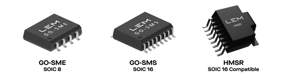
Thermal Performance Considerations for Integrated Current Sensors
LEM’s ICS devices operate in ambient temperatures from –40 °C to +125 °C, up to +150 °C for certain models. In addition to ambient conditions, self-heating from primary current dissipation must be managed — the sensing element is positioned very close to the primary conductor, so heat buildup can directly impact junction temperature. Exceeding the maximum junction temperature (Tj max = 165°C) must be strictly avoided.
The maximum junction temperature results from the combination of:
- Ambient temperature
- Self-heating due to conductor resistance (Joule heating)
Thermal performance is a balance between:
- Primary lead frame cross-section — Larger cross-sections lower resistance and reduce heating.
- Primary constriction — Narrower cross-sections improve magnetic coupling, increasing sensitivity and reducing noise.
Example temperature rise at 40 A:
- GO-SME: ~95.6 °C max
- GO-SMS: ~57.7 °C max
- HMSR: Optimized for higher peak currents (up to 25 kA) while maintaining safe Tj.
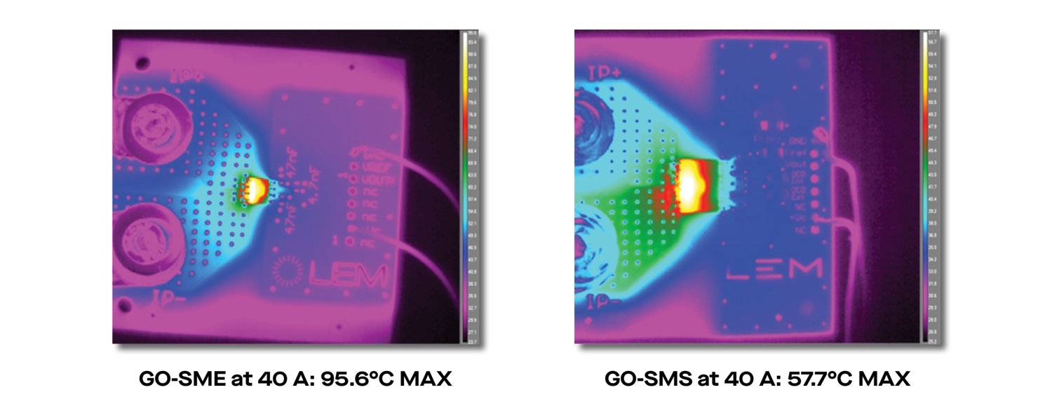
Recommendation: Perform thermal simulations and physical measurements in the final PCB assembly to ensure worst-case Tj remains below 165 °C.
Setting Passive Components for ICS Filtering & Stability
LEM’s Current Sensor ICs require a set of external passive components for optimal operation.
| Function | Typical Value | Purpose | Notes |
|---|---|---|---|
| Output Filter Capacitor (Vout - GND) | 47 nF | Smooths high-frequency noise | X7R recommended for thermal stability; in limited temp. range (industrial use), cost optimized caps acceptable |
| OCD Filter Capacitor (OCD - GND) | Not Required | Response time is internally defined | External capacitor does not prevent false triggering |
| Voltage Divider Resistors (OCD threshold) | R1 + R2 ≈ 200 kΩ | Sets OCD trip point using Vref | High value ensures low current drain on Vref while maintaining accuracy |
| Pull-Up Resistor (fault pin) | 4.7 kΩ – 10 kΩ | Ensures valid logic when fault inactive | Value depends on MCU input specs |
Programming the Over-Current Detection (OCD) Threshold
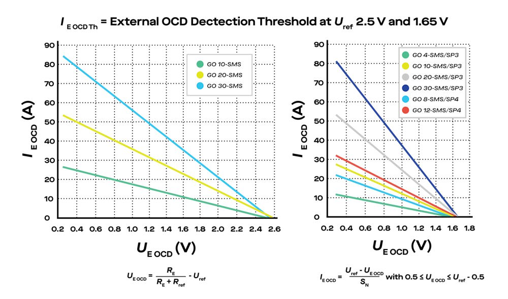
The OCD pin allows for hardware-level current limit configuration without firmware changes.
How it works:
- Integrated Current Sensors generates an internal voltage proportional to measured current
- This voltage is compared to the OCD pin voltage
- OCD pin voltage is derived from Vref through a resistor divider
Divider formula:
VOCD = Vref x R2 / (R1 + R2)
Example:
- Vref = 2.5 V
- Desired trip point = 80% of nominal current → Vout = 2.0 V
- Select R1 = 10 kΩ, R2 ≈ 15 kΩ to achieve 2.0 V at OCD pin
Best Practices:
- Use precision resistors (±1% or better)
- Ensure divider current ≥ 100 µA for stable operation
- For field adjustments, only R2 needs to be changed
Additional Pins & Functions
- OCD Internal – Factory-set threshold comparator for fixed over-current protection; use as a backup layer.
- Fault Pin – Open-drain output, low during over-current; connect to MCU to interrupt or shutdown circuitry.
- Test/Calibration Pins – For factory use; typically left unconnected in end products unless specified.
- Vref Pin – Provides stable reference voltage, often 2.5 V, for OCD programming and MCU’s ADC reference; decouple with 100 nF placed close to the pin.
Enhance Over-Current Protection with LEM Current Sensor IC Integration
By combining thoughtful PCB routing, correct passive component selection, and precise OCD programming, designers can fully leverage LEM’s Current Sensor ICs capabilities.
Following these integration guidelines ensures:
- Accurate, stable measurements
- Reliable over-current protection
- Robust performance in noisy industrial environments
Due to their integrated architecture and straightforward implementation, LEM Current sensor IC offer a seamless path from concept to deployment. Their ease of integration not only accelerates time-to-market but also reduces design complexity, making them ideal for both high-volume industrial applications and agile prototyping environments. With minimal external components and intuitive configuration, integrated current sensors solutions empower engineers to focus on building smarter, safer systems with minimal design overhead.